Samsung Electronics will be the first business in the world to mass-produce second generation (1y-nano) 10nm-class DRAMs. Compared to current first generation (1x-nano) 10nm-class DRAMs, number of chips that can be produced from single wafer will be increased by whopping 30%.
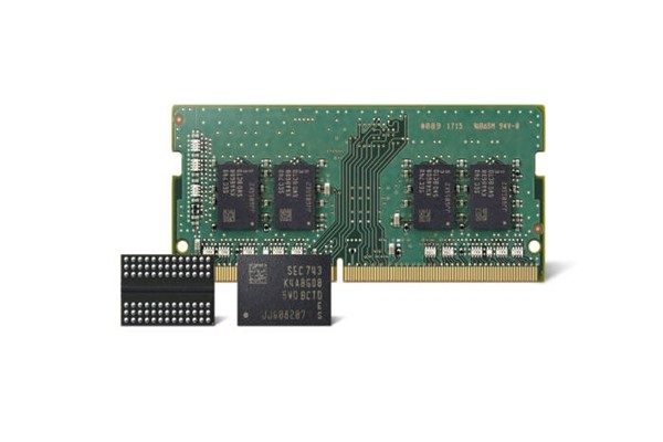
Samsung Electronics made an announcement on the 20th that it started mass-producing 1y 8Gb DDR4 DRAMs starting from last month. Samsung Electronics opened a generation for first generation 10nm (1x-nano) DRAM in February of 2016 and it was able to overcome limitations of refining process in just 21 months.
New DRAM is applied with innovative technology for its design. DRAM is able to differentiate 0 from 1 by detecting whether or not electric charge is stored inside a capacitor. 8 billion capacitors are installed within a 8Gb DRAM. However a problem arises when an area of floor of a capacitor, which needs to store certain amount of electric charges, needs to be reduced when line width is refined. In order to maintain space for storage while reducing an area of floor, capacitors needs to be designed higher. In such case, capacitors may tilt and either become attached to an adjacent capacitor or crumble in a worse case scenario. Reason why refinement of DRAM has become slower recently is because it is difficult to solve such problems regarding design of capacitors.
Samsung Electronics drastically reduced size of capacitors. Reduced size of capacitors also leads to reduced amount of storage of electric charges which indicates that it is difficult to differentiate 0 from 1. However Samsung Electronics applied data sensing system based on super-high sensitive amplification technology so that DRAM can clearly differentiate 0 from 1 even if amount of electric charges that are stored is reduced.
Experts expect that this sensing system will become an innovative technology that will solve future problems regarding refinement of DRAM process. A representative for Samsung Electronics also explained that this sensing system will become a ‘game changer’.
Second generation DRAM is also applied with second generation air gap technology. Air gap is a technology that fills very small area next to bit line where current flows with air that has excellent insulation effect rather than a particular substance. By doing so, it is possible to minimize amount of unnecessary electric charges that are stored and develop super-high sensitive cells. This air gap technology also improves degree of integration of cell arrangement and it can drastically reduce size of chips that makes 30% improvement in productivity possible. 1y DRAM is 10% faster than 1x DRAM and consumes 15% less electricity than 1x DRAM.
“We were able to overcome limitations in refinement of semiconductors by developing innovative technologies with changed thinking.” said President Jin Kyo-young of Samsung Electronics Memory Business Department. “We are planning to enhance our competitive even more in the future by entirely changing premium DRAM markets to 10nm-class DRAM markets through increased production of 1y-nano DRAMs.”
Samsung Electronics is planning to target next-generation premium DRAM markets such as DDR5 for servers, LPDDR5 for mobile devices, HBM3 for supercomputers, and GDDR6 for super-fast graphics with 1y DRAM. 1y-nano DRAM module already completed packaging evaluation done by CPU companies.
Staff Reporter Han, Juyeop | powerusr@etnews.com