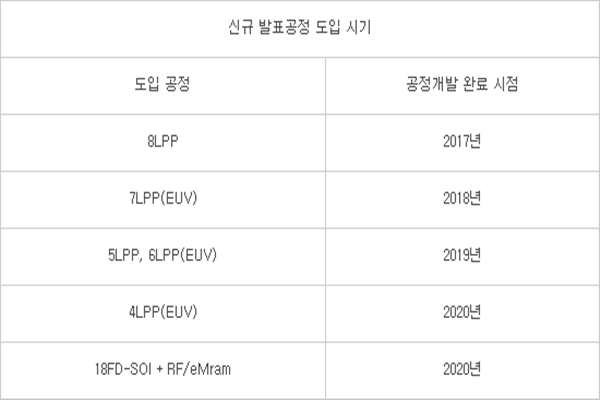
Samsung Electronics introduced a roadmap for introduction of high-tech 4-nano system semiconductor foundry process in 2020. It is going to commercialize 8-nano process, 7-nano process, and 6-nano and 5-nano process in 2017, 2018, and 2019 respectively. It is going to embed MRAM memory into 18-nano FD-SOI (Fully Depleted – Silicon On Insulator) as a technology that will produce low and middle-priced chips and is planning to complete a platform that will combine RF (Radio Frequency) function and embedded MRAM memory. This platform will be commercialized in 2020.
Samsung Electronics announced such roadmap at ‘Samsung Foundry Forum’ that was held in Santa Clara on the 24th (U.S. time). This forum is the first event that was held after Samsung Electronics officially declared establishment of ‘Foundry Business Department’ during a reorganization of Samsung Electronics DS sector on the 12th of this month and had about 400 people from its customers and partners in attendance.
Samsung Electronics introduced that 8-nano LPP (Low Power Pus), which will be commercialized this year, is practically the last micro process that can be implemented through current immersion exposure apparatus before introducing EUV (Extreme Ultraviolet) exposure apparatus. It is likely that 7-nano LPP, which is planned to be commercialized in 2018, will be the very first logic process that introduces EUV apparatus. Samsung Electronics emphasized that it will overcome limitations of current micro processes by working with apparatus manufacturer called ASML from Netherland. It is predicted that 6-nano LPP, which will be introduced in 2019, will be based on 7-nano process and will increase degree of integration and characteristic of low power. It seems that 5-nano LPP, which is planned to be commercialized in 2019 along with 6-nano LPP, will be the last micro process that can be implemented through current FinFET (Fin Field Effect Transistor) gate structure.
GAAFET (Gate All Around FET) structure, which is one step more advanced than FinFET, will be applied for the first time for 4-nano LPP which is planned to be commercialized in 2020. Samsung Electronics has named this technology MBCFET (Multi Bridge Channel FET). Major principle of this technology lies on the fact that shape of gate path where current flows changes from quadrilateral FinFET structure to a cylindrical structure.
Although current flows from 3 sides of FinFET, GAA can have current flow to every sides that cover a cylinder. If path where current flows becomes wider, performance also increases accordingly. Another characteristic of GAA is that it is relatively easy to reduce width.
28-nano FD-SOI process for customers that produce low and middle-priced chips was also introduced. FD-SOI is a process technology that greatly reduces current from getting leaked by forming oxide films on top of a wafer. Samsung Electronics introduced a platform that combines embedded MRAM memory and RF technology to 28-nano FD-SOI. This platform is currently being mass-produced. It announced its plan to expand this platform to 18-nano FD-SOI in 2020.
“Roles of semiconductors are becoming bigger during ‘hyper-connected generation’ where every devices are connected.” said Vice-President Yoon Jong-shik of Samsung Electronics Foundry Business Department. “As a foundry business that possesses roadmaps for extensive high-tech processes, we are going to provide optimum customized solutions by actively establishing partnership with our customers.”
Starting with this Foundry Forum in the U.S., Samsung Electronics is going to continue to hold other events in South Korea and other countries.
Staff Reporter Han, Juyeop | powerusr@etnews.com