KAIST (Korea Advanced Institute of Science and Technology, Chairman Kang Seong-mo) has developed a technology that can easily manufacture micro and nano structures and it is going to apply this technology to high-integrated nano semiconductor process within couple years.
KAIST made an announcement on the 8th that a research team led by Professor Kim Hee-tak of Bio Chemical Engineering Department has developed a new ‘imprint lithography’ technology that can manufacture more detailed micro and nano structures by preventing expansion and contraction of heat.
Imprint lithography is based on a concept where nano structures are made by filling materials that are going to be patternized inside of mold and it is seen as an important technology for variety of fields such as electronics, optical science, and surface science. Until now semiconductor industries could not make accurate nano structures due to distortion in pattern because they had used a method that expands raw material by applying heat or UV in order to fill raw material into mold. When temperature drops, materials that are patternized will contract and lose their original shape.
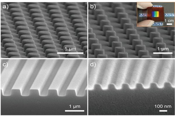
Research team utilized ‘azobenzene’ as a patterning material and allowed micro and nano structures to be printed even in room temperature. Azobenzene has a property to liquefy and flow towards where light is shot. If light is shot from the top, it can even shoot up to 3 micrometers vertically.
Research team manufactured small structures without any expansion and contraction of heat by placing transparent mold on top of azobene and shooting light on top of it and succeeded in manufacturing structures that are smaller than 100 nanometers. Team also manufactured complicated structures that are combined with different scales.
Nano structures can be made with other materials that are mixed with azobenzene because azobenzene maintains its properties even in mixed state.
Research team explained that this technology can be utilized in variety of fields such as manufacturing of semiconductors and optical science and is planning to develop a technology that can manufacture even smaller nano structures in the future. Its first goal is to secure technical skills that will can manufacture 50 nanometer structures within couple years. These skills can be applied to high-integrated nano semiconductor process.
“By utilizing azobenzene’s vertical direction movement, we were able to manufacture nano structures that are smaller than 100 nanometers.” said Professor Kim. “We have improved imprint lithography technology by one step higher.”
Staff Reporter Kim, Youngjun | kyj85@etnews.com