The age of inspection through 3D X-Ray right at the spot where semiconductor has been produced has come. World’s first ever nano level semiconductor processing from production to inspection is happening.
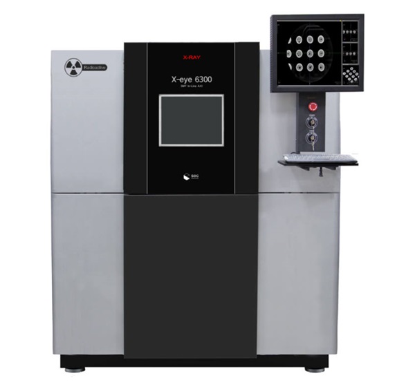
Sec has announced on the 30th that they have created industrial inspectional X-Ray machine ‘X-eye 6300’ that has advanced inspection speed and accuracy.
When the inspection objected semiconductor is put in the middle of this machine, it spins 360 degree while taking hundreds of X-Ray shots. Then it combines the pictures together into 3rd dimensional image and finds flaws. It is the same method as CT scan used in hospitals.
The machine recognizes flaws accurately down to 600 nanometer level, which is 1/167 of a hair thickness. They have solved problem of not being able to find flaws to nano level with 3D X-Ray. It is world’s finest technology that even competitors in Germany or Japan had not succeeded in developing.
It merely takes 3 seconds from X-Ray shooting, image producing, and analyzing. Because it only takes 3 seconds to inspect, the X-Ray inspection equipment may be used in the production line directly unlike before.
Ever since the recent semiconductor packaging has been changed to layer form, 3D inspection method has found flaws even to soldering parts in between the semiconductors that the previous 2D method could not.
Sec said they had developed the machine through their X-Ray producer ‘tube’ manufacturing technology. The company’s machine can materialize degree to 200 nano meter.
Sec Representative Jonghyun Kim said, “Korea has been using imported industrial X-Ray inspection machine but now we have domestically produced and made it to the top in the domestic market. We will be showing the product for the first time at the ‘NEPCON KOREA 2015’ that will be held in COEX starting on the 3rd.”
Staff Reporter Yoo, Changsun | yuda@etnews.com